Next-Generation Lithography: An Efficient Choice for Fabrication
Next-generation lithography (NGL) refers to techniques that use short-wavelength lights to help achieve finer resolution features from existing light wavelengths. The need for NGL stems from the drive towards chip sizes of 5nm and beyond.
There are many potential candidates of NGL, like Extreme Ultraviolet (EUV) lithography, x-ray lithography, electron beam lithography, focused ion beam lithography, and nanoimprint lithography, of which EUV is a leading candidate owing to its high throughput, wide processing window, and extendibility to small feature size, and cost-effectiveness.
What’s Next-Generation Lithography?
Semiconductor chip manufacturers are moving towards next-generation chips with 7 nm and beyond. The lower fabrication technology allows the manufacturers to integrate more components in the reduced wafer area, increase speed, and reduce power consumption. Next-generation lithography techniques aid in realizing the next-generation chips with extremely low geometries.
NGL techniques use a shorter wavelength than conventional lithography techniques. Potential candidates for NGL are Extreme Ultraviolet (EUV) Lithography, X-ray lithography, Electron Beam Lithography, Focused Ion Beam Lithography, and Nanoimprint Lithography.
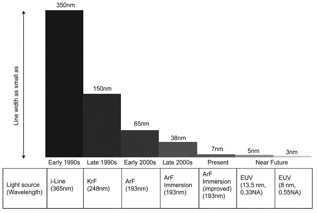
EUV Lithography is the leading candidate for NGL owing to its high throughput, wide processing window, extendibility to small feature sizes, and cost-effectiveness. EUV Lithography is the leading candidate for the NGL technique owing to its high throughput, wide processing window, extendibility to small feature sizes, and cost-effectiveness. However, at higher resolutions, EUV Lithography still faces many challenges related to scanners, photo-resists, masks, etc.
The EUV ecosystem faces its worst supply shock in a decade, with a significant share of global helium supply offline and buffer stocks hovering at just 4–10 weeks. Alternative routes must materialize within the next two months; without them, advanced-node production in key semiconductor hubs will slow down. This is not a supply chain risk to monitor; it is an operational issue demanding immediate action. – Deepak Kumar Jain, Industrials, Hi-tech, and Mobility Leader, Stellarix
Extreme Ultraviolet Lithography (EUV): Overview, Advantages, Drivers, and Challenges
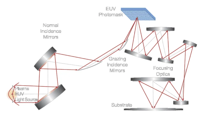
Extreme ultraviolet lithography (EUV) is an optical technique used for modern chip fabrication that enables chip manufacturers to print modern chips on silicon wafers at the scale of 7nm, 5nm, and below. Moreover, EUV utilizes a high-energy ultraviolet light source at 13.5nm wavelength. The generated extreme ultraviolet light focuses on a reflective EUV photomask with the help of multiple mirrors. The reflective photomask bounces the extreme ultraviolet light to the silicon substrate covered by the layer of photoresist material to transfer the integrated circuit design to the silicon substrate.
It entered mass commercial production in 2018 and is an optimal and efficient choice for fabricating modern integrated circuits for applications like 5G, AI, autonomous vehicles, IoT, Industry 4.0, etc. It is available for both logic and DRAM chips. Further, the increased adoption of DRAM projects increases the overall demand for EUV.
However, there are several potential challenges in implementing this technology:
- EUV tools must be operated within a vacuum environment, as the radiation cannot be transmitted into the ambient air.
- All solid materials strongly absorb EUV radiation, so conventional refractive optics are impossible, and reflective masks and imaging systems must be used.
- The efficiency of the light source for EUV lithography continuously degrades, impacting chip yields or causing failures.
To overcome the challenges related to EUV light source efficiency, industry players are using a high-power source of EUV light with an anamorphic projection system, which improves the throughput to 180 wafers per hour and overall cost efficiency. The EUV Lithography market is expected to register a CAGR of 15% by the year 2026. ASML is the dominant player in the market and has made considerable strides towards precise and efficient production of semiconductors at small transistor scales, around 7nm node size or even 5nm. It holds a monopoly in manufacturing and supplying EUV Lithography machines.
ASML Holding’s EUV Lithography Portfolio: Overview, Product Portfolio, Future Roadmap
ASML is an innovation leader in the semiconductor industry. Its lithography solutions have been making giant leaps on a “tiny scale” since 1984. Their technology, hardware, and software together provide a holistic approach to mass-producing patterns on silicon.
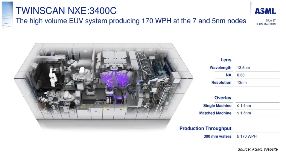
ASML’s current product line comprises TWINSCAN NXE3400B, TWINSCAN NXE: 3400C, and TWINSCAN NXE: 3600D. Using a wavelength of 13.5 nm, ASML’s EUV systems pattern the finest lines on microchips. In fact, they are used in high-volume manufacturing to create the highly complex foundation layers of the most advanced microchips (7, 5, and 3 nm nodes).
ASML’s TWINSCAN NXE: 3400B started shipping in 2017 and supports EUV volume production at the 7 and 5 nm nodes. The TWINSCAN NXE: 3400C, the successor to the NXE: 3400B, supports EUV volume production at the 7 and 5 nm nodes at higher productivity. The TWINSCAN NXE: 3400C includes improvements in the EUV source industrialization, overlay, focus, and productivity. It came into commercial use in the second half of 2021.
The TWINSCAN NXE: 3600D is ASML’s latest-generation lithography system, supporting EUV volume production at the 5 and 3 nm Logic nodes and leading-edge DRAM nodes. The TWINSCAN NXE: 3600D combines imaging and overlay improvements with a 15% to 20% productivity improvement capability compared to its predecessor, the NXE: 3400C.
Working on Development
ASML is working on the development of a high numerical aperture (NA) EUV lithography product line. The high NA EUV lithography system is the next step of the current system based on the .33NA lens. In the near future, ASML plans to launch a high NA EUV lithography system with a .55 NA lens capable of handling an 8nm wavelength compared to the current 13.5 nm wavelength. EUV 0.55 NA higher resolution will enable 1.7x smaller features and 2.9x increased density. Further, EUV 0.55 NA’s higher imaging contrast enables a 40% improvement in local CDU and improves productivity on critical layers. ASML also plans to launch the .55 NA EUV tool with a target of 3nm wavelength by 2025.
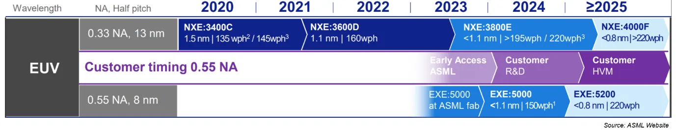
Figure 4 indicates the roadmap of ASML’s product lines in the EUV space for 0.33 NA and 0.55 NA. The NXE: 3800E and EXE: 5000 are in the development phase, whereas the NXE: 4000F and EXE: 5200 are in the definition phase 14.
The Race of Foundries
TSMC, Samsung, and Intel are the leading foundries competing in the EUV Lithography space. As a result, all three companies are part of the original investors in lithography equipment vendor ASML and have purchased multiple EUV lithography systems. Currently, TSMC is dominating the semiconductor manufacturing foundry business.
The following are a few critical points of the three leading players:
- TSMC has approximately 50% of all the active EUV machines installed worldwide
- TSMC also has several, approximately 60% for cumulative EUV wafer production
- Samsung is the world’s second-largest foundry player, with an estimated market share of 18% in the first quarter of 2021. It currently has 25 EUV scanners, about half the quantity owned by its bigger rival, TSMC10.
- In October 2020, Samsung ordered 20 EUV scanners from ASML
- For 3-nanometer and finer process nodes, Samsung is planning to adopt its skill, known as gates all around (GAA) technology, as demand for advanced chips is growing with the take-off of artificial intelligence, 5G, and autonomous driving10
- Intel has invested in ASML’s “High NA” EUV Machine, EXE: 5000, to regain its position as a maker of the smallest and fastest chips from TSMC12
Next-generation Lithography: Conclusion
EUV Lithography has enabled several foundries to produce chips at 7nm and 5nm. Chip scaling boosts the performance of DRAMs, FPGAs, GPUs, and processors. Further, AI, automotive, servers, and wireless systems need faster chips with more functions.
The industry will focus on R&D in EUV, which will help pave the way for current and future devices. In R&D, the industry is developing new EUV scanners, masks, and resists for the following nodes. 3nm is slated for 2022, followed by 2nm a year or two later. Nonetheless, it will require massive funding and time to develop future EUV technologies.
Let's Take the Conversation Forward
Reach out to Stellarix experts for tailored solutions to streamline your operations and achieve
measurable business excellence.