3D additive electronics have received a lot of attention in the past few years due to their effectiveness in enabling on-demand manufacturing of highly customizable electronics on a broad variety of substrates and conformal surfaces. Additively manufactured electronics offer a potent alternative to buffer manufacturing with their rapid designing, prototyping, manufacturing process and higher volume production. Some manufacturing technologies, such as carbon digital light synthesis, aerosol jet, and hydro-printing; are used in the manufacturing of additive electronics. Further, incorporation of advanced materials will boost the efficiency and versatility of additively manufactured electronics. Electronics manufacturing companies, such as Nano Dimension, Cubbison Company, Molex LLC, Pasternack Enterprises Inc, and Optomac, are focusing on their technical improvements.
Additive Electronics or additively manufactured electronics is an industry production name for electronic devices manufactured using 3D printing or additive manufacturing techniques. Additive manufacturing methods, generally used for mechanical parts, have been integrated with advanced electronics production technology to enable the highly flexible fabrication of customized 3D electronic devices.
The technique is compatible with photonic structures. However, it will frequently need higher dielectric and conductive element printing resolutions. Further, its capacity to integrate multiple materials in a single print job is extremely useful.
Conventional v/s Additive Electronics
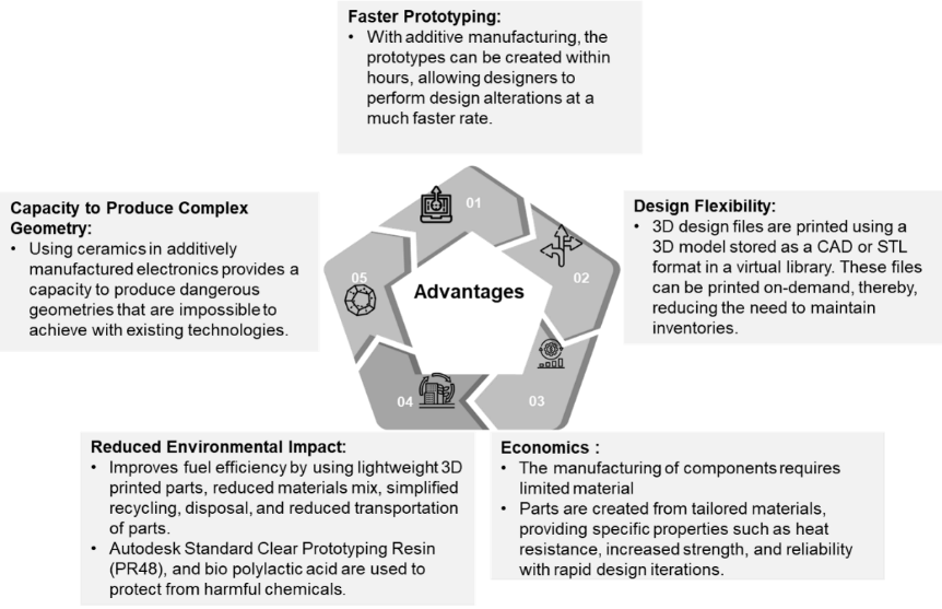
Additive electronics provide advantages over traditionally manufactured electronics. These include faster prototyping, reduced lead time, cost savings, and reduced errors. They also offer increased integration, customization, on-demand production, better finishing, and optimized design. Electronic components are manufactured by deposition of layer-by-layer material in precise geometric shapes. This process utilizes data from computer-aided design (CAD) software or 3D object scanners.
Market Activities
Active research and development activities in material and photonics are the major elements driving the development of additive manufacturing in electronics.
Developing new polymers enables the fabrication of electrical sensors, passive elements, piezoelectric actuators, and MEMS elements. Microfluidics is also used in this process. Photonics development allows circuits to be printed at higher resolutions and miniaturized sizes.
Several market players are developing advanced electronic solutions, such as flexible integrated circuitry, prosthetics, customizable batteries, sensors on uneven surfaces, etc., with the help of additive manufacturing in electronics.
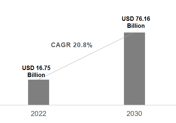
The overall market for additive electronic manufacturing is estimated to reach USD 76.16 billion by 2030 at a CAGR of 20.8%.
Commercialization of Additively Manufactured Electronics
Nano Dimension is the most active player in this field. It is working with a number of collaborators to develop additively manufactured electronic products. The most noteworthy activities of Nano Dimension are summarized below.
- Nano Dimension and ProtoSpace UTS (an additive and advanced manufacturing facility at the University of Technology Sydney) have developed 5G devices like multi-layer linear polarization (LP) patch 5G antenna elements as well as 22 LP antenna arrays using the DragonFly LDM 3D printing equipment, without altering the array’s size or profile, this feeding network is integrated into the same substrate as the antenna array element.
- Nano Dimension acquired DeepCube, a firm developing machine learning algorithms, to establish a distributed electronic fabrication network based on machine learning. The technology provides Nano Dimension digital management over its global network of 3D printers, which can self-learn and increase their efficiency over time.
- Nano Dimension and the Fraunhofer Institute for Manufacturing Engineering and Automation (Fraunhofer IPA) developed innovative freeform 3D printing and assembly procedures to manufacture electromechanical systems.
IP Activities
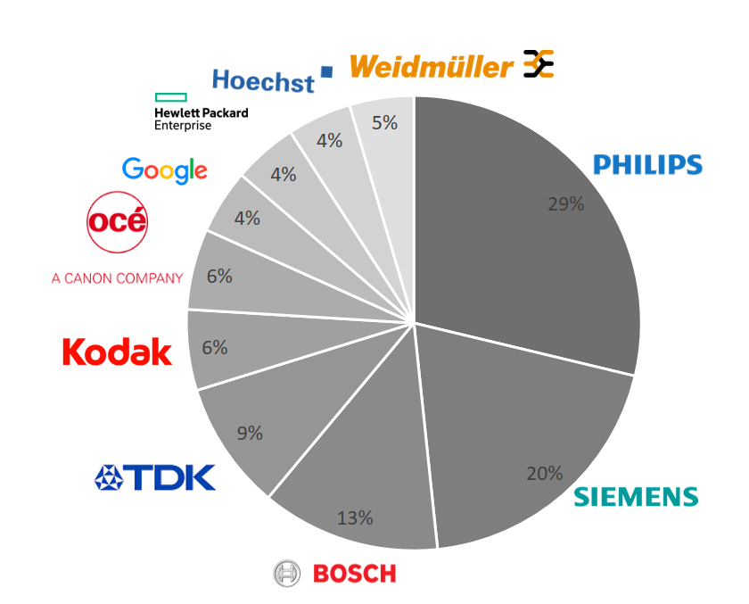
The below-given chart below shows the patents filed by the top assignees in the 3D additive electronics domain. The chart shows that Philips is the major assignee with the highest filings, followed by Siemens, Bosch, and TDK corporations.
Manufacturing Technologies
- Carbon DLSTM 3D Printing Technology: Carbon Digital Light Synthesis TM (Carbon DLSTM) is a revolutionary resin-based 3D printing technique that produces polymeric items with superior mechanical qualities, resolution, and surface quality using digital light projection, oxygen-permeable optics, and engineering-grade materials.
The technology enables previously unachievable designs. It allows for fast manufacturing and production. It provides massive capacity and strong quality assurance. The parts produced have unrivaled durability, resolution, and polished surface.
- Aerosol Jet Technology: Aerosol Jet Technology is being used to print electronic components like resistors, capacitors, antennas, sensors, and thin-film transistors. Here, the components are printed directly onto 3D surfaces, eliminating the need for a separate substrate and lowering the product’s size, thickness, and weight. The technology is also being used to develop antennas and sensors that fit the contour of the underlying substrate, such as a phone cover. Additionally, nanoparticle inks have been tuned to Aerosol Jet technology to allow printing onto plastic substrates at low heat deflection temperatures.
- Hydro-Printing Technology: Hydro-printing is a technique for transferring ultrathin, transparent, double-sided conductive nano-membranes. The technique is used for multiscale conformal electronics. It finds applications in soft robotics component fabrication. It is also used in 3D electronics and communication devices like Near Field Communication (NFC) antennas.
Incorporation of Advance Material
- Plastic (for example, ULTEM™ 9085 resin) is the most often used 3D printing material because it has advantages such as being lighter than metal equivalents for electronic components in industries such as automotive and aerospace where weight is a problem, and its proper management can yield better fuel economy.
- Conductive ink is applied in layers on a substrate to create micro-interconnect structures, eliminating the need for high-temperature operations and lowering manufacturing costs. It also increases the number of high-resolution devices with high metallic conductivity.
- Polyethylene terephthalate glycol (PETG) and acrylonitrile butadiene styrene (ABS-T) have average mechanical, thermal, and dielectric properties. They are used during Fused Filament Fabrication (FFF) during additive manufacturing, making them appropriate for low-demanding electronic applications.
Future Aspects
Cutting-edge technologies like deep learning and artificial intelligence can aid in innovating new electronic products. These products can have improved miniaturization, nano-geometries, 3D structures, on-demand manufacturing, and digital inventory—for example, using Femtosecond (FS) lasers to enhance solar cell efficiency. FS lasers are used to modify the surfaces of solar panels. The process involves creating periodic structures. These structures have nano and microscale features. The surface texturing is performed on black silicon.
Conclusion
Researchers and the electronics industry have gained interest in additively manufactured electronics in recent years. This is due to the focus on customization, cost efficiency, and environmental impact reduction of electronic components. Also, the use of additive manufacturing offers several advantages. These include the elimination of raw material wastage, eco-friendly processes and products, and faster component optimization.
This electronic device manufacturing technique has the potential to become a game changer. It is already revolutionizing several fields and industries. Applications such as 3D embedded electrical devices, 3D conformal electronics, and flexible and stretchable electronics are transforming how things are done. With further enhancements in this technology, manual assembly procedures for attaching components on PCBs can be reduced. In addition, this will lead to shorter development times for working prototypes and finished products.