5G is the successor of the 4G LTE network. The 5G network spectrum is divided into two types: mmWave spectrum, and sub-6GHz spectrum. The 5G infrastructure market is very dynamic and requires significant strategic decisions from equipment providers, semiconductor chip manufacturers, service providers, and regulatory bodies to create a fast and efficient network. Gallium Nitride (GaN) is a potential solution to overcome the challenges related to thermal management in network equipment, efficient antenna material with larger bandwidth, and faster front-end RF signal processor chips with linear performance at higher temperatures.
The 5G Era
With the increasing demand for connectivity and mobility in the current networked society, 5G technology has the potential to fulfill the demands with increased speed, seamless mobility, and low latency. The transition to 5G technology comes with the adoption of higher frequencies like sub-6 GHz and mmWave (>20 GHz) bands. As 5G deployment and adoption are in the transition phase, parallel technologies like signal processing, semiconductor technologies, printed circuit boards, antenna designs, and material choices are in transition too. The industry players are working hard to deploy 5G infrastructure using smart materials for 5G operation. However, at every level, 5G infrastructure presents challenges and great opportunities.

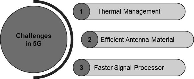
Some of the major challenges faced while operating at higher frequency bands are thermal management, efficient antenna material, faster signal processors, etc.
Smart Materials For 5G Operation: Thermal Management
5G uses shorter wavelength signals, which allows for smaller antenna sizes and the production of more densely packed antenna arrays, as well as densely packed arrays of power amplifiers and beamforming electronic components.
Extreme thermal conditions exist within the highly integrated components in a small area due to the densely packed array of antenna elements, power amplifiers, and beamforming electronic devices. The challenges associated with thermal conditions can be addressed using high-performance material-based technologies.
Efficient Antenna Materials
With the mmWave technology, 5G enables massive MIMO technology to serve more terminals at the same frequency band, which increases the number of RF chains per installation, beamforming capabilities, and the number of antenna elements used at the base stations. The utilization of higher frequencies with massive MIMO raises the data transmission rates and channels while reducing the signal propagation range and increasing the transmission losses due to interference with objects such as buildings, trees, rain, etc. In order to overcome the challenges with higher frequencies and massive MIMO, there is a need for an improved radiating antenna element that can dynamically and efficiently adjust the transmission power and beamforming patterns.
Materials For 5G Operation: Faster Signal Processing Chips
5G technology uses sub-6 GHz as well as mmWave (28 – 41 GHz) frequency bands for greater data rates, bandwidth, and lower latency, which allows the implementation of many applications like augmented reality (AR), virtual reality (VR), artificial intelligence (AI), internet of things (IoT), factory automation, vehicular communication, etc.
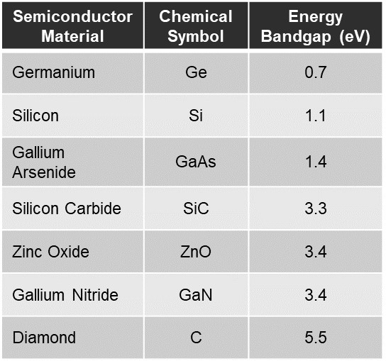
For all the 5G applications, the complexity of the front-end RF transceiver module is increasing. As the MIMO capacity increases, more filters get added to the signal-processing modules. The signal processing chips fabricated with lower bandgaps of conventional semiconductor materials, such as germanium, silicon, gallium arsenide, etc., struggle with efficiency at higher frequencies. The front-end RF transceiver modules fabricated with lower bandgaps of conventional semiconductor material also face thermal issues due to the large difference between peak and minimum power requirements. Wide bandgap materials that can efficiently handle higher voltages in a smaller area can overcome the challenges of efficiency and heat issues in front-end RF transceiver modules.
Material Needed in 5G
Key industry players are working around the clock to overcome the challenges of thermal management, efficient power transmission, accurate beamforming, processing efficiency, etc.

The major hurdle for solution providers is managing intense thermal conditions while enclosing the components in a small area, along with excellent performance at minimal power. These issues can be resolved with the development of high-performance materials.
Electronic devices fabricated with compound materials by combining III-V semiconductor materials such as GaN, GaAs, SiC, ZnO, and others will outperform electronic devices fabricated with conventional CMOS technology for high-frequency 5G mmWave applications. These compound semiconductor materials offer high substrate resistivity, electron mobility, power gain ratio, reduced noise, and lower body effects, making them suitable for the fabrication of high-frequency 5G mmWave electronic devices.
GaN as a Semiconductor Material for 5G
GaN offers an energy bandgap of 3.4 eV, which makes it suitable for fabricating electronic devices for 5G mmWave applications. Along with the higher energy bandgap, GaN also offers an improved power and packaging density that allows the manufacturing of highly dense antenna arrays, power amplifiers, and beamforming circuitry.
GaN Performance Advantages
- GaN offers a higher power density, which is its primary advantage. GaN-based power amplifiers also allow for smaller form factors, which require less PCB space.
- The enhanced power efficiency of GaN also leads to lower base station operating costs.
- GaN shows an increased thermal dissipation performance (it can work at 250 F) that decreases the overall system size and cost with simplification of heat-sink designs and cooling needs.
- GaN’s high-frequency and wide-bandwidth efficiency assist in the reduction of massive MIMO systems.
- GaN devices are easily scalable to high output power as they offer high output impedance with lower parasitic capacitance.
- Excellent high-voltage sustainability
Materials For 5G Operation: GaN on Si vs GaN in SiC
5G solutions need to incorporate technologies that can deliver performance, efficiency, and value requirements. Gallium Nitride (GaN) has emerged as a vital solution that can meet these requirements. There are two solutions for RF applications utilizing GaN: Gallium Nitride (GaN) on Silicon (Si) and Gallium Nitride (GaN) on Silicon Carbide (SiC).
Both of the solutions offer individual advantages as well as disadvantages. A few of the major points are mentioned below:
- Thermal Conductivity: GaN on SiC offers three times the thermal conductivity than GaN on Si, allowing the device to run at a higher voltage and power density.
- Efficiency: GaN on SiC offers better efficiency in the high-temperature environment of the wireless infrastructure, while GaN on Si suffers from temperature changes as Si is highly resistive at room temperature and conductive at high temperatures.
- Cost: The cost of growing GaN epitaxy on silicon is more than that of GaN epitaxy on SiC, offering significant efficiency and a cost advantage over GaN on Si.
Future Innovations – 5G and GaN
It can be predicted that GaN’s impressive power density capabilities will improve in the upcoming years. Techniques to attain better power density with GaN exist today, but the costs for those techniques are so expensive that they haven’t been commercially viable. For example, GaN might be used on diamond instead of silicon carbide. It is feasible, but the cost makes it unfeasible for base stations.

GaN-based solution providers must collaborate closely with telecommunication system designers to develop innovative techniques to cool embedded system elements. This strain will be even greater in smaller outdoor units with massive MIMO arrays. Today, many alternatives are available, but they are not inexpensive.
For the telecommunication sector, the increased linear power of GaN-based semiconductor devices is the top priority for industry players. Industry players do not expect major changes in modulation techniques, signal processing, and transceiver circuitry at the base station in the future. GaN-based solution providers in the industry aim to eliminate trapping effects as much as feasible to make systems as simple as possible.
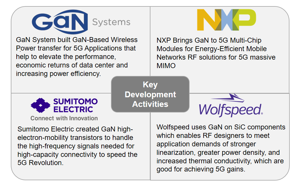
GaN Systems, NXP Semiconductors, Wolfspeed, Mitsubishi Chemical, Kyocera, Plessey Semiconductors, IQE, MonoCrystal, Sumco, Sumitomo Electric, Hitachi, and DowCorning are among the major companies working on the development of GaN-based solutions for 5G infrastructure applications. The following are some companies’ key development initiatives.
Materials For 5G Operation: Conclusion
GaN offers good performance for 5G sub-6 GHz and mmWave applications due to its high energy bandgap, high voltage resistance, low energy loss, thermal dissipation capability, and other characteristics. GaN will play an important role in applications related to 5G technology, such as front-end RF signal processing, antenna element designs, power amplifiers, beamforming processors, etc.
In the near future, the number of installations for 5G base stations with sub-6 GHz and mmWave will grow at an exponential rate. With the installations, the demand for high-performance and efficient networking equipment will grow, driving industry players to continuously improve GaN-based solutions to deliver efficient and high-performance solutions at a low cost.